Simplify Your Printed Circuit Board Making
There are many different types of Printed Circuit Board materials in the market these days. The common ones are FR-1, FR-2, CEM-1, CEM-3 and FR-4 . The thickness of the PCB can be 1.0mm, 1.2mm or 1.6mm. They can be single sided or double sided with cooper clad of 1 oz or 2 oz.
These are the common low cost PCB that electronics hobbyist or students can use for their projects. Of course there are more complicated multilayer PCB that are used in the industry for various applications.
If you are an electronics hobbyist or students who are tight on the budget of making Printed Circuit Board, how do you make your own printed circuit board? If you were like me, I used to go through the many processes in making the PCB a few years ago.
I used to make the PCB layout, print the layout on a suitable transparency (one that can withstand the temperature of the laser printer and photocopy machines), use of photo-resist chemical (require a dark room to do this) on the PCB to ensure that the PCB pattern can be transferred to the PCB, transfer the layout from the transparency to the PCB by the use of ultra violet light, use of developer to develop the pattern on the PCB, etched the developed pattern on the PCB, washed the PCB, drilled the required holes, mount the components and solder the components.
Over the years, I have found out that with the advancement of technology, there are better ways to do the Printed Circuit Board processes. It helps to eliminate the use of darkrooms, photo-resist chemical, developer chemical, negatives/transparency, ultra violet lights and long waiting time to cure the photo-resist.
In simplifying the making of PCB, the direct benefit of this is it reduces the cost needed to set up the PCB making facilities.
The items below are the simplified steps of making simple single sided or double sided PCB for electronics hobbyists, students, or even electronics designer.
PCB Layouts
You will start by making a layout of the PCB by using a CAD software such as Eagle, Protel, Orcad and other suitable software. Of course there are lots of PCB layout of various projects that you can get from electronics magazines or CAD software. However, I find it more rewarding and one learns more by putting your hands on the available CAD software.
To do the layout yourselves, you need to draw the schematics and after that the PCB layout. Eagle, Altium and Autotrax EDA are some of the software that you can use to do the layout.
Printed Circuit Board Design Rule
There are a few things to look out for when one does the PCB layouts. It is important to take note that the layout must take into consideration the cost factor as well as the practicality of making the PCB in-house. Listed below are some of the design rule that one should try to adhere while doing the PCB layouts. The detailed EMC(Electromagnetic compatibility) aspects will not be covered here.
PCB Electrical Clearance, Track Width Rules
In the PCB design of electronics circuit, it is important that one plan and has a checklist of the do's and don'ts before proceeding to do the printed circuit board layout. The understanding of the circuit is critical to the design, for example one needs to understand the maximum current and voltage that are carried by each conductor in order to determine the track width of the conductor and the type of PCB that will be used. Some examples of the IPC standard are provided here.
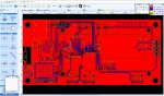
PCB Prototypes
Once the PCB layout has been completed, one can start thinking of transferring the layout from the CAD software or even the layout from electronics magazines. The author would like to suggest that one jump over the steps of using transparency, photo-resist chemical, developer chemical and the use of Ultra Violet light. The use of Printed Circuit Board Transfer Film will eliminates the steps mentioned.
If your layout is in the CAD software, just print the layout onto this transfer file using a laser printer. If your layout is in the form of hard copy like magazines or artwork, all you need to do is to photocopy the layout into the PCB transfer Film.

Recent Articles
-
Electronics Design Contest
 Join electronics design contest and win prizes. Test your hardware and software skills against the best designers from the rest of the world.
 -
Garden Watering Circuit
 Experiment and test out this automatic garden watering circuit that will detect the moisture of the soil and on or off the water valve accordingly.
 -
Electronics Events
 Join the electronics events to enhance your knowledge and network with other professionals in this industry.
Design and build a battery tester to test dry cell and rechargeable battery with a voltage of less than 2V. Check here.
PCB Prototypes
Make your own printed circuit board and learn the processes involved along the way. More here.
Learn how to dissipate heat from your heat-sensitive electronic components.
Test the reliability of your products to the environment by stressing them in test lab.
Explore the use of 7-Segment Display, 555 Timer, Decade Counter and Binary Adder. Get the circuit.
Construct this simple door bell chime and have fun. Find out more here.
Build this simple home alarm to protect your house from intruders. See the schematic circuit.
New! Comments
Have your say about what you just read! Leave us a comment in the box below.