FMEA of Electronic circuit
INTRODUCTION TO FMEA ON STRESS DERATING
This article recommends the criteria of FMEA in the area of stress derating of electrical and electronics parts or components and indicate the maximum application stress values to consider during design of electronic circuits. Derating is increasing the ratio of the margin of safety between part design limits and the allowable applied stresses.
Derating provides extra protection for part tolerances and decreases the part degradation rate and by this it increases the life expectancy of a part.
The margin of safety of a part to both the threshold and time dependent stresses are generally unknown. As such, parts should be derated to the maximum extent possible depending on the maximum environment of which the parts are subjected to.
During derating, one must consider the manufacturer's parts environmental specifications and the operating conditions of the application and then apply the derating factors so as not to exceed the maximum allowable application stresses set forth in this document.
Take note that this is a typical design recommendation and designer should use their own discretion when applying using this FMEA document for their references.
EXAMPLE OF FMEA DERATING CALCULATION
A carbon film resistor which is rated at 2 Watts at 20 °C, linearly derating to zero at 85 °C being used in a machine rated at 60 °C. Find whether the rating of this device is suitable to be used or otherwise.
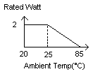
Step 1: Calculate rated power at 60 °C
P(60 °C) = P(25 °C) X [(Tmax - Toperating)/(Tmax - Trating)]
= 2 X [(85-60)/(85-25)]
= 0.83 W
Step 2: Find out the recommended maximum allowable stress from the table below - limit the power to 0.50
Maximum P allowed at 60 °C = 0.50 X 0.83 W = 0.415 W
Step 3: From the schematic design, find out the maximum power applied to the resistor. For example if the value of the resistor is 100 ohm and the maximum current applied is 0.05 Ampere, the power consumed is (0.05X0.05) X 1,000 W = 0.25W.
Step 4: The maximum power consumed(0.25W) is less than the maximum allowable derated power(0.415 W) and therefore it is safe to use the rated resistor in this application.
The table below shows the common components that are used and the recommended allowable FMEA derating factor.
| Type of components | Critical Stress | Maximum allowable Stress factor |
|---|---|---|
| a) Fixed resistors | ||
| i) Carbon | Power | 0.50 |
| ii) Film insulated | Power | 0.50 |
| iii) Wirewound power | Power | 0.50 |
| b) Variable resistors | ||
| i) Wirewound | Rated current | 0.70 |
| ii) Non wirewound | Rated current | 0.70 |
| iii) All types | Voltage | 0.80 |
| c) Thermistor | Power | 0.50 |
| d) Capacitors | ||
| i) Ceramic | Voltage | 0.50 |
| Current AC/Ripple | 0.70 | |
| Surge | 0.70 | |
| ii) Paper | Voltage | 0.50 |
| Current AC/Ripple | 0.70 | |
| Surge | 0.70 | |
| iii) Plastic | Voltage | 0.50 |
| Current AC/Ripple | 0.70 | |
| Surge | 0.70 | |
| iv) Tantalum, foil or film | Voltage | 0.50 |
| Current AC/Ripple | 0.70 | |
| Surge | 0.70 | |
| v) Air | Voltage | 0.30 |
| e) RFI Filters | Current(steady state) | 0.75 |
| Voltage(steady state) | 0.75 | |
| f) Transformer/chokes | Insulation Breakdown voltage | 0.50 |
| Current | 0.70 | |
| g) Diodes | ||
| i) Recifier circuit | Power | 0.30 |
| Surge current | 0.50 | |
| Forward current | 0.50 | |
| Peak Inverse voltage | 0.50 | |
| ii) Switching | Power | 0.30 |
| Surge current | 0.50 | |
| Forward current | 0.50 | |
| Peak Inverse voltage | 0.50 | |
| iii) SCR | Power | 0.30 |
| Surge current | 0.50 | |
| Forward current | 0.50 | |
| Peak Inverse voltage | 0.50 | |
| iv) General Purpose | Power | 0.50 |
| Surge current | 0.50 | |
| Forward current | 0.50 | |
| Peak Inverse voltage | 0.50 | |
| v) Zener | Power | 0.50 |
| Forward current | 0.50 | |
| vi) ALL types | Junction temperature | 110 °C |
| h) Transistors | ||
| i) Power | Power | 0.30 |
| Current | 0.70 | |
| Voltage | 0.70 | |
| ii) Switching | Power | 0.50 |
| Current | 0.70 | |
| Voltage | 0.70 | |
| iii) General Purpose | Power | 0.50 |
| Current | 0.70 | |
| Voltage | 0.70 | |
| i) Voltage Regulators | Max. rated Input voltage | 0.80 |
| Max. rated Output current | 0.75 | |
| Max. rated Power dissipation | 0.60 | |
| j) Digital Integrated circuit | Output current | 0.80 |
| Operating freq | 0.75 | |
| k) Connectors | Contact current | 0.60 |
| Working voltage | 0.25 |

Recent Articles
-
Electronics Design Contest
 Join electronics design contest and win prizes. Test your hardware and software skills against the best designers from the rest of the world.
 -
Garden Watering Circuit
 Experiment and test out this automatic garden watering circuit that will detect the moisture of the soil and on or off the water valve accordingly.
 -
Electronics Events
 Join the electronics events to enhance your knowledge and network with other professionals in this industry.
Design and build a battery tester to test dry cell and rechargeable battery with a voltage of less than 2V. Check here.
PCB Prototypes
Make your own printed circuit board and learn the processes involved along the way. More here.
Learn how to dissipate heat from your heat-sensitive electronic components.
Test the reliability of your products to the environment by stressing them in test lab.
Explore the use of 7-Segment Display, 555 Timer, Decade Counter and Binary Adder. Get the circuit.
Construct this simple door bell chime and have fun. Find out more here.
Build this simple home alarm to protect your house from intruders. See the schematic circuit.
New! Comments
Have your say about what you just read! Leave us a comment in the box below.