PCB Design Layout Rules Recommendation
In the PCB design of electronics circuit, it is important that one plan and has a checklist of the do's and don'ts before proceeding to do the printed circuit board layout. The understanding of the circuit is critical to the design, for example one needs to understand the maximum current and voltage that are carried by each conductor in order to determine the track width of the conductor and the type of PCB that will be used.
The voltage difference between each track will determine the clearance between each conductor. If the clearance is not enough, chances are that the electrical potential between each track will cause spark over and short circuit the PCB.
This will cause functional failure to the product and the safety of the users that are using the product will be compromised. It is therefore critical for one to understand some of this basics requirements before one proceed to design the PCB.
Tracks Restricted Area
Tracks should not be located on the areas that can caused them to be peeled off easily. One of the restricted area is holes on the PCB which are used to mount screws or PCB spacers. These holes are usually used to secure the PCB to a casing or to secure it in a fixed place.
The edges of the PCB should not have any tracks as these areas are usually used to transport the PCB from one process to another process by using a conveyor belt. These edges are places where the possibility of scratches and cracking of the PCB happens. The recommended areas that should not have any track is as shown in the diagram below assuming a hole diameter of 4 mm which is used to mount a PCB spacer.

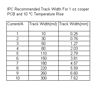
Conductor Thickness and Width
The PCB conductor thickness and width will determine the current carrying capacity of the track. The IPC standard for the conductor thickness and width of the common 1 oz/square-feet PCB is as shown below. However, it is always advisable to use a bigger value due to the tolerance and variation of the PCB processes. If higher current carrying capacity is required, a 2 oz/square-feet or 3 oz/square-feet type of PCB is preferred. Many electronics hobbyist prefer to solder a thick cooper conductor on the PCB track to increase the current carrying capacity of the track.
PCB Design Electrical Clearance
Many safety standards call for a minimum of 8mm clearance between 40V mains and other isolated signal tracks. These safety standards are to ensure that the users that are using the products will be protected from any electrical hazards.
For non main voltages, IPC recommend the electrical clearance between adjacent tracks. It is important to know the maximum difference in voltage that are applied on the adjacent tracks of a PCB. The electrical clearance specs of IPC standard is as shown below for various condition of the PCB.
Coating the PCB will help to reduce the requirements of the track clearance. However, the quality of the coating as well as the material used are critical to ensure that these requirements are met. Again, it is always advisable to increase the clearance to cater for the variations of the PCB processes.

Recent Articles
-
Electronics Events
Join the electronics events to enhance your knowledge and network with other professionals in this industry. -
Electronics Design Contest
 Join electronics design contest and win prizes. Test your hardware and software skills against the best designers from the rest of the world.
 -
Garden Watering Circuit
 Experiment and test out this automatic garden watering circuit that will detect the moisture of the soil and on or off the water valve accordingly.
Design and build a battery tester to test dry cell and rechargeable battery with a voltage of less than 2V. Check here.
PCB Prototypes
Make your own printed circuit board and learn the processes involved along the way. More here.
Learn how to dissipate heat from your heat-sensitive electronic components.
Test the reliability of your products to the environment by stressing them in test lab.
Explore the use of 7-Segment Display, 555 Timer, Decade Counter and Binary Adder. Get the circuit.
Construct this simple door bell chime and have fun. Find out more here.
Build this simple home alarm to protect your house from intruders. See the schematic circuit.
New! Comments
Have your say about what you just read! Leave us a comment in the box below.