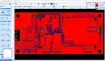
PCB Design Rule Simplified
The followings are the suggested PCB design rule that you should try to adhere to in order to minimize the cost of fabricating the PCB. This design rule is specifically done for electronics enthusiasts as well as students who are still not familiar with the fundamentals of PCB design and layouts.
a) Single Sided PCB and PCB material
As far as possible, one should try to layout the PCB to single sided layer as far as possible. It may be quite difficult to rout the PCB but with the use of jumpers, you should be able to rout most of the simple circuity into single sided PCB. Of course at times you may need to use double sided PCB and multilayer PCB.
The use of double sided PCB will increase the price to 1.5 to 2.5 times compared to single sided PCB. Common single sided PCB thickness is 1.6mm, 1 oz cooper clad, CEM-1 or FR-2 materials. As far as possible, try to use FR-2 which is paper phenolic type of PCB material. This is by far among the cheapest PCB that is used in most consumer electronics products today.
b) Panelisation of PCB
The PCB laminates normally comes in standard sizes. One of the common PCB laminates come in dimension of 40 inches X 48 inches. In order to maximise the use of the PCB, you should find out from the manufacturers the standard PCB sizes that they are using. By effective panelisation of the PCB, you can use up to 80%-90% of the PCB laminates.
This will reduce the cost of each PCB. If the layout panelisation is not effective, wastage up to 50% may occurred. Therefore, always check the effective panelisation of PCB before sending for fabrication.
If you are doing the prototyping yourself, this PCB Design Rule applies as well.
c) Size of the PCB
You should try to make use of the smallest area of the PCB as possible taking into consideration the track width, spacing and other constraints. Always try to minimise the size of PCB during the layout of the PCB. The size of the PCB is critical being the fundamental of the PCB Design Rule.
d) Reduce the number of holes and vias
Whether you send the PCB for CNC (computer controlled PCB drilling) or you drill the holes yourself, you should try to reduce the number of holes and vias on the PCB. Since the time utilised by the machine will determine the price of the PCB, the lesser holes and vias will reduce the cost of the PCB. The rule is to keep it simple and as basic as possible.
e) Reduce the number of types of holes sizes
Try to design with common hole size as much as possible. This is to avoid changing the drill bits used by the machine. By having many types of hole sizes, the machine will have to change the drill bits and this takes time. The time taken will determine the cost of the PCB. Common drill bits sizes are 0.7mm, 0.8mm, 0.9mm, 1.0mm, 1.2mm, 1.5mm, 2.0mm and 3.0mm.
f) Track Width and track spacing
For your own prototying or even sending out for PCB houses for fabrication of the PCB, it is always advisable not to design the track width and track spacing to the limit of the manufacturercapabilities. For instance, if you need to design 0.3mm track width, try to use 0.5mm.
Similarly if the minimum track spacing needed is 0.3mmm, use 0.5mm instead. This will help to ensure that the yield is high during the production of the PCB. This PCB Design Rule is especially critical if you are fabricating the PCB on your own.
g) Silkscreen minimisation
If top overlay silkscreen is required, the PCB Design Rule recommend that you do not need to silkscreen the bottom overlay. It may be difficult to do trouble shooting later on but eliminating this process will save some cost as well.
Back To PCB Design Rule Home Page

Recent Articles
-
Electronics Events
Join the electronics events to enhance your knowledge and network with other professionals in this industry. -
Electronics Design Contest
 Join electronics design contest and win prizes. Test your hardware and software skills against the best designers from the rest of the world.
 -
Garden Watering Circuit
 Experiment and test out this automatic garden watering circuit that will detect the moisture of the soil and on or off the water valve accordingly.
Design and build a battery tester to test dry cell and rechargeable battery with a voltage of less than 2V. Check here.
PCB Prototypes
Make your own printed circuit board and learn the processes involved along the way. More here.
Learn how to dissipate heat from your heat-sensitive electronic components.
Test the reliability of your products to the environment by stressing them in test lab.
Explore the use of 7-Segment Display, 555 Timer, Decade Counter and Binary Adder. Get the circuit.
Construct this simple door bell chime and have fun. Find out more here.
Build this simple home alarm to protect your house from intruders. See the schematic circuit.
New! Comments
Have your say about what you just read! Leave us a comment in the box below.