Electronic Design Circuits Touch Switch
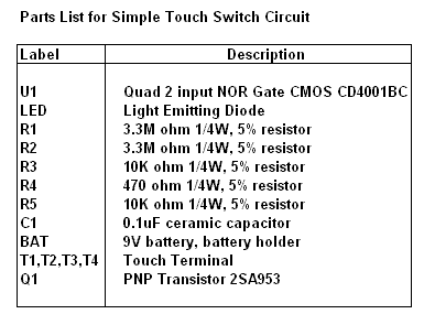
In this electronic design circuits touch switch project, a CMOS quad 2 input NOR gate IC is used as a latching circuit to switch a LED ON and OFF by physically touching the ON metal plate or OFF metal plate. The CD4001BC integrated circuit is a monolithic complementary MOS (CMOS) IC that are constructed with N- and P- channel enhancement mode transistors. Its input are protected against electrostatic discharge with diodes to VDD and VSS.
The circuit below shows the schematic diagram of the touch circuit of which the NOR gates are configured as a simple latching circuit. When the skin contact is made between contacts T1 and T2 or T3 and T4, the LED switches ON and OFF respectively. The latching circuit is to ensure that the output will not fluctuate between ON and OFF.
When the T1 and T2 contacts are bridged through the skin contact, the output of U1-a will go to logic "0" and caused the output of U1-b to go to logic "1". This output will in turn caused NOR gate U1-c to go to logic "0" causing transistor Q1 to turn ON, and hence LED will turn ON.
The circuit will remain latched with the LED ON until contacts T3 and T4 are bridged of which the output of U1-a will go to logic "1", output of U1-b will go to logic "0", output of U1-c will go to logic "1" and the transistor Q1 will turn OFF. The LED will then turn OFF.
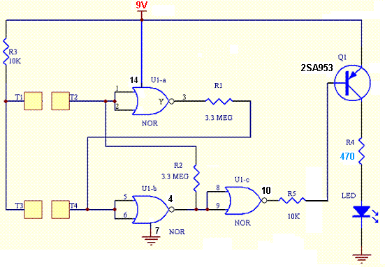
It is important to ensure that 9V battery is used as its DC source. If you use the mains supply to step down the voltage using a transformer for rectification and filtering to get the 9V DC supply, ensure that the transformer is designed in such a way that it follows the safety standard requirement of UL. This is important to ensure the safety of the user that is using the metal contacts to ON/OFF the LED.
Electronic Design Circuits Touch Switch Home Page

Recent Articles
-
Electronics Events
Join the electronics events to enhance your knowledge and network with other professionals in this industry. -
Electronics Design Contest
 Join electronics design contest and win prizes. Test your hardware and software skills against the best designers from the rest of the world.
 -
Garden Watering Circuit
 Experiment and test out this automatic garden watering circuit that will detect the moisture of the soil and on or off the water valve accordingly.
Design and build a battery tester to test dry cell and rechargeable battery with a voltage of less than 2V. Check here.
PCB Prototypes
Make your own printed circuit board and learn the processes involved along the way. More here.
Learn how to dissipate heat from your heat-sensitive electronic components.
Test the reliability of your products to the environment by stressing them in test lab.
Explore the use of 7-Segment Display, 555 Timer, Decade Counter and Binary Adder. Get the circuit.
Construct this simple door bell chime and have fun. Find out more here.
Build this simple home alarm to protect your house from intruders. See the schematic circuit.
New! Comments
Have your say about what you just read! Leave us a comment in the box below.